Characterisation
of 42-10 CCDs
This short note summarises some of the basic tests performed on the three initial 42-10 devices. The three devices were "off the shelf" devices purchased from EEV (now Marconi) to test the response of 42-10's for ionising and non-ionising radiation. Before these tests were started, a few initial characterisations of the CCD were made. These characterisations are described below.
It should be noted that this document is not a test report, merely a compilation of some of the initial familiarisation tests on the CCDs and electronics. Consequently, the results are not reported in the same depth (eg with full details of led types, etc.) which would be expected in a comprehensive test report. The following images and graphs are thus provided for information only.
The three CCDs are all front-illuminated and are in a dual-in-line ceramic package. Currently, the test camera cannot be cooled and so all of the measurements are at room temperature (about 20 °C).
Three devices are used: serial numbers as follows:
8352-14-1
8352-16-1
8351-6-1
1 Basic image properties
Serial number - 8352-14-1
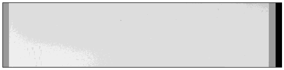
Figure one below shows a one second image of a test target (the UCL/MSSL logo) placed directly above the CCD. Light emitting diodes were used for illumination. A dark current image has been subtracted. Image size is 2048x512 pixels.
 Figure
one
Figure
one
Figure two shows a half second image of a USAF test target with dark current subtracted. Image size 2048x512.
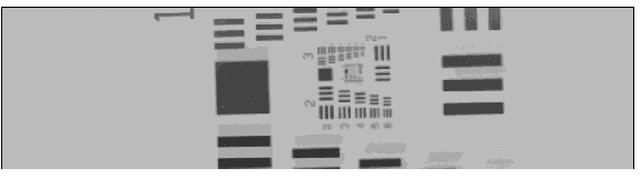
Figure Two.
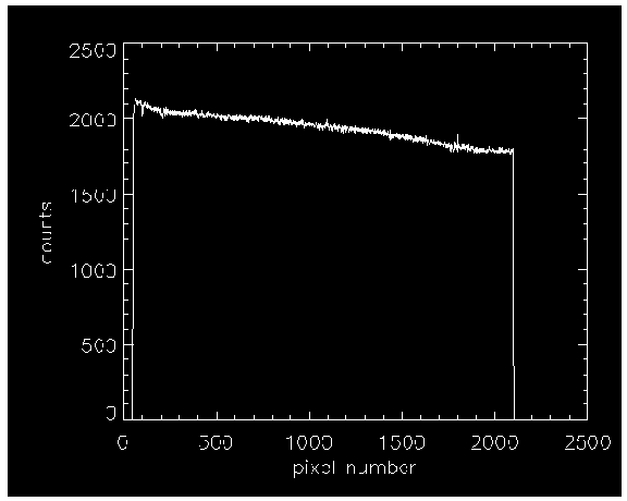
Figure three shows a line plot through the central row (row 250) of the CCD.
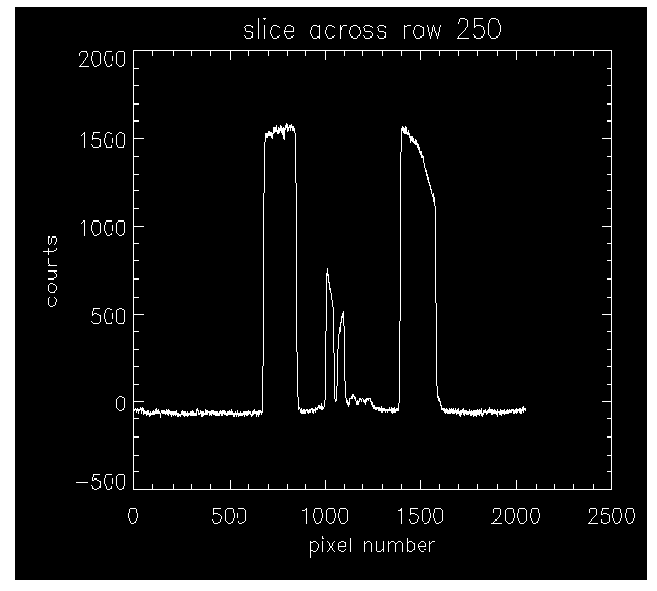
Figure
three.
CCD serial number:s/n - 8352-16-1
|
|
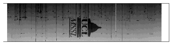
Figure s four and five show a one second image of the UCL/MSSL logo test target. For illumination one led at 4mA was used, on for 0.5s. Figure four includes dark current subtraction, figure five has no dark current subtraction.
Figure four
|
|

Figure
five.
Figures six and seven show a one second image of the USAF test target. For illumination one led was operated at 4mA for 0.5s. Figure six shows the test target with no dark current subtraction, figure seven with dark current subtraction.
|
|
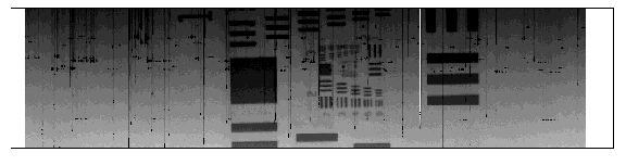
Figure six.
|
|

Figure seven
CCD serial number: 8351-6-1
Figures eight and nine show images obtained using the same test targets. Dark current has been subtracted from both images
|
|
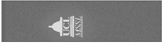
Figure eight
|
|
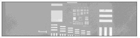
Figure nine
CCD Imaging Resolution
The resolution of the CCDs varied depending upon illumination conditions. Using the line pair groupings on the USAF test target it was possible to resolve down to about group 3,5 which has a line spacing of 12.7 cycles per mm, corresponding to around 80µm.
Figure ten shows a plot of an image taken of a USAF test target. There are four bars shown, increasing from pixel zero:
group 4,4 (22.6 line pairs per mm)
group 4,3 (20.1 line pairs per mm)
group 4,2 (17.9 line pairs per mm)
group 4,1 (16.0 line pairs per mm)
|
|
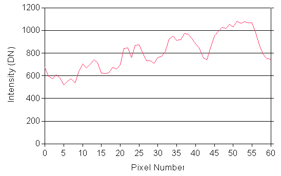
Figure ten
The separation between the elements of group 4 is clearly visible, but it is not possible to easily make out the three members of each element.
Linearity of the CCDs
It was intended to verify the linearity of the 42-10 CCDs up to the full well capacity. The response of the CCD to linear increases in intensity from an led was measured. The intensity of the led was increased, by increasing the driver current, and the corresponding electrons within a 10x10 area of the CCD. Unfortunately the 12 bit response of the camera in high gain mode is not sufficient to digitise up to the full ~120k full capacity, and so the linearity of the CCD could only be tested up to ~90k electrons. A plot of linearity (up to about 90k electrons) is shown below in figure eleven.
|
|
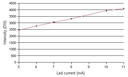
Figure eleven
2 Flat field
The purpose of the flat field characterisations was two fold. Firstly, to try and establish an optimum number and position of light emitting diodes which will provide a flat field and secondly, to see how flat fields taken with the three CCDs compare.
Flat field measurements were initially taken using CCD serial number 8352-14-1. Images were taken with four and six diodes respectively. The diodes were approximately positioned either about 40mm above the CCD or about 100mm above the CCD. The diode currents were adjusted to give an approximate level of 1000 DN, corresponding to about 24000 electrons (the camera has a gain of 24 electrons/DN).
A current of around 5mA at 3V was used. Initially, variation across the face of the CCD varied as orientation was altered, but it was reasonably straightforward to achieve a good flat field across the CCD once the diodes were perpendicular to the front face of the CCD. Once this position was found, small variations in position (a displacement of 1mm of so) made little difference to the flat field. In addition, adjustment of position from 100mm to 40mm did not require a large adjustment in current to maintain a flat field at about a quarter full well.
The flat field measurement is taken using six diodes, at 5mA. The diodes are one for 0.3s and the image is taken for 0.5s. There is no dark current subtraction.
Serial number: 8352-14-1
Figure twelve shows the flat field obtained with the diodes at 100mm above the CCD with a current of 5mA at 3V.
|
|
Figure
twelve.
Figure thirteen below shows a line profile plot through row 250.
|
|
Figure
thirteen
CCD serial number: 8352-16-1
Figure fourteen below shows the flat field from a 0.3s diode illumination, current 4mA. There is no dark current subtraction.
|
|
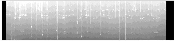
Figure fourteen.
Figure fifteen shows the same flat field, but with a dark current subtraction.
|
|
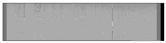
Figure fifteen
Figure sixteen shows a plot through row 250 of the dark subtracted flat field.
|
|
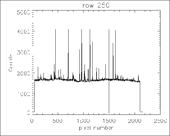
Figure sixteen
Variation in flat field values
Although the aim is to achieve as flat a field as possible, it is most important to ensure that the measurement to measurement variation in flat field is low. Figure seventeen shows the variation for nine successive flat field measurements. The values plotted are the mean pixel count rate within a 100 pixel by 20 row area. Although on the full scale, the variation from measurement to measurement looks small, a noticeable step function can be seen when the axis scale is decreased.
|
|
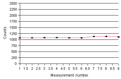
Figure Seventeen
|
|
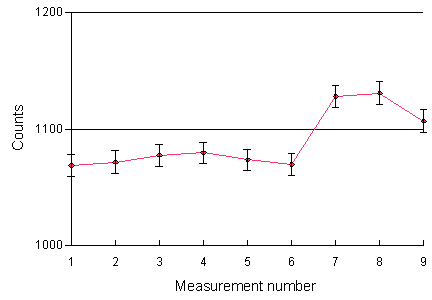
Figure eighteen, the flat field variation displayed in figure
seventeen, but over a shorter axis range.
Distribution of hot pixels and image defects
An estimation of the number of image defects for the flat fields was made by obtaining the three sigma value of the median pixel intensity, and then highlighting all the pixels with intensities higher and lower than this three sigma value. Using the three sigma values removes any dependency on image position for the pixel position (as there is a definite decrease in intensity across the image).
8351-14-1
Median intensity - 1919 (with dark current subtraction).
Value of 3s = 364
Number of pixels above 3 s = 954
Number of pixels below 3 s = 949
8351-16-1
Median intensity - 1743
Value of 3s =2022
Number of pixels above 3 s = 6283
Number of pixels below 3 s = 0
The variation in this image is so large that the three sigma value falls bellow zero.
3 Estimation of CTE
values
One method for estimating the charge transfer efficiency values is to measure the amount of charge in the overscan pixels at the end of the image. In theory, the value of these overscan pixels should be that corresponding to a zero signal. Any additional charge which is measured in these pixels will represent charge that has been "deferred" from other pixels within the image.
Any deferred charge was measured by imaging a flat field, and then examining the overscan pixels for indication of "deferred "charge. Additional counts above the zero level were seen, as in figure nine below. However, this "deferred" charge also exists in the fifty lead in pixels at the start of the image, which is cannot have been caused by deferred charge. One possibility for this extra charge is that the amplifier in the current camera can not cope with swings from a large amount of charge to none at all, and that some settling time is required.
Figure seventeen shows the variation in count rate for the last 100 pixels in row 250. Although there should be a sharp transition from white to black, the counts decrease slowly over a number of pixels. Potentially, this could be a sign of poor charge transfer efficiency but figure eighteen shows that a similar increase in charge occurs in the first 100 lead in pixels. This argues against the presence of deferred charge in the CCD.
|
|
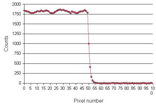
Figure ninteen
|
|
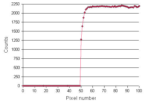
Figure twenty
The most likely explanation is that the electronics are having trouble coping with transitions from white to black and from black to white. However, a CCD simulator is available which outputs a large number of black/white lines to the ROE (shown in figure twenty one). Tests with this CCD simulator show that this is not the case as the ROE appears to be able to handle the transition within one pixel (shown in figure twenty two) with only a very brief difference between the first pixel in a block and subsequent pixels.
|
|

Figure twenty one
|
|
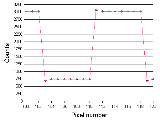
Figure twenty two
4 Dark noise
Initial measurements taken with the camera were all at room temperature and consequently, for the non MPP devices measured here, the dark noise was high.
The following plots (figures twenty three and twenty four) show a comparison of the dark noise for 8351-14-1, which shows good image cosmetics, and 8352-16-1 which has
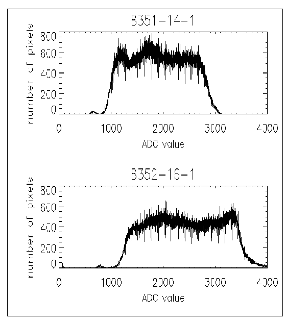 Figure twenty three
a large number of hot pixels and cosmetic defects. Due to the large number of hot pixels in 8352-16-1, the full dark noise for this CCD is not shown in this figure twenty three, but is shown in figure twenty four.
|
|
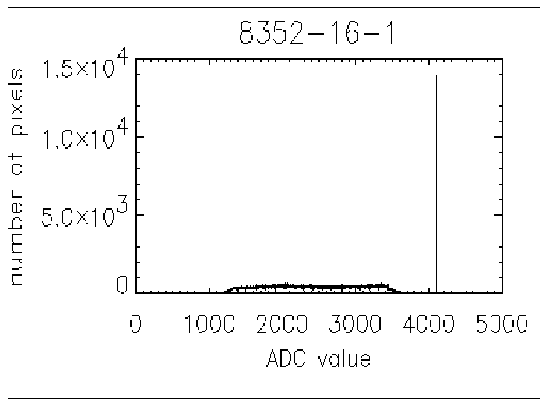
Figure twenty four
Variation of dark noise with substrate voltage
The value of dark noise obtained will vary with the substrate voltage. As the substrate voltage decreases, the CCD will come out of inversion. Consequently, the surface traps will no longer be filled by the holes from the channel stops, and the dark noise will increase dramatically. This can be shown below in figure twenty five for both CCD 8352-16-1 and 8351-6-1. The values for the dark counts have been calculated by integrating all counts over a 500 pixel square area. Both CCDs show the expected behaviour, with dark noise increasing as the substrate voltage is reduced. Images of the dark noise were viewed for both CCDs (particularly 8352-16-1) to see if there was any noticeable difference in image quality with different substrate voltages, but no discernable difference could be seen.
|
|
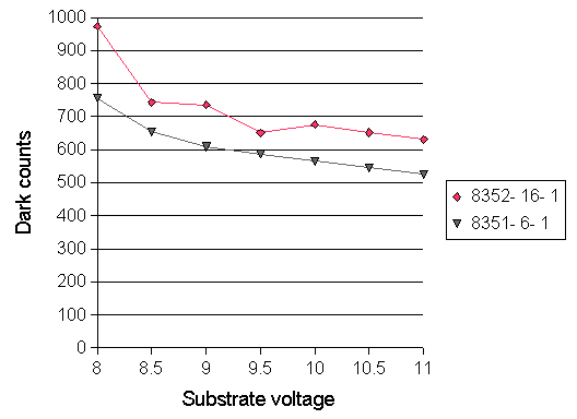
Figure twenty five