Charge Dithering (also known as 'charge sloshing') is a way of reducing the dark noise of a non-MPP (Multi pinned phase) CCD so that it has a value similar to that which would be obtained with an MPP device.
The majority of the dark current generated within a CCD occurs at so called 'surface states' which exist at the boundary between the Si-Si02 interface. This dark current can be reduced by suppressing the surface states by operating the CCD in 'inverted mode' whereby negative voltages (with respect to the substrate) are applied to the imaging phases, driving each phase into inversion. The negative charge attracts holes which fill up the surface states, suppressing dark current generation. However, a positive potential must exist under one of the electrodes (to be able to attract photo-generated electrons) which means that substantial dark current will be generated under this phase.
An MPP CCD is one solution to this problem: an additional implant under one of the phases means that all three phases can be held low during integration, completely suppressing the dark current generation by the surface states.
A second solution to suppressing the dark current without resorting to using an MPP CCD is to use dither clocking during integration.
If an electrode phase is dithered by being periodically taken in an out of inversion at a rate faster than the lifetime of the surface state traps then these traps will effectively remain filled whilst the imaging phases are dithered. The lifetime of the surface states traps is strongly dependent on the temperature. For example, at room temperature a dither rate of around 50µs should be sufficient to produce MPP-like dark current. At lower temperatures, MPP-like dark current can be achieved using just several dithers during an integration.
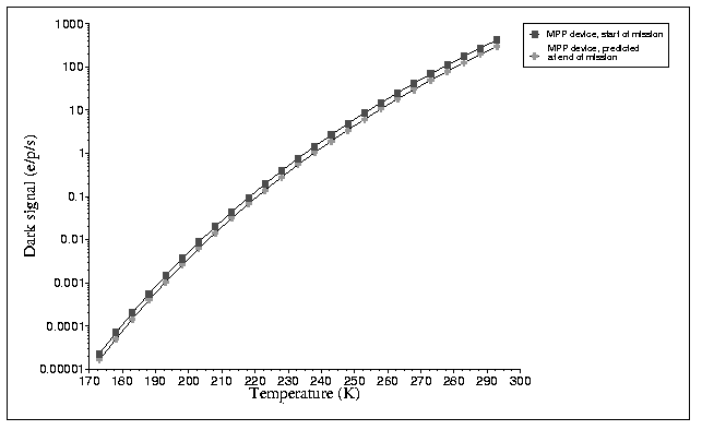
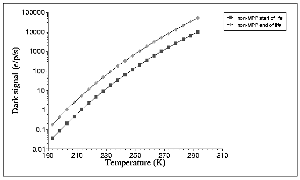
Typical dark current values for both MPP and non-MPP devices are shown below.
At first sight, it would appear that an MPP device is the optimum choice. However, there are both advantages and disadvantages in selecting either an MPP or non-MPP device. Some of these are described below:
MPP devices
advantages
· better dark current characteristics without requiring dither clocking;disadvantages
· hence, easier electronics;
· marginally better radiation tolerance;
· lower full well capacity ~90k electrons compared with ~120k for non-MPP (for the Marconi 42-10 CCD);Non-MPP devices
· slightly lower clocking speeds are possible;
· no supplementary buried channel is possible for the 42-10 device - hence likely to have higher Charge Transfer Inefficiency (CTI).
advantages
· larger full well;disadvantages
· some higher complexity required to implement 'dither clocking' to reduce dark current to MPP levels;A measurement of the dark current suppression obtained when using dither clocking was made at MSSL using a Marconi Applied Technology CCD 42-10. The measurements were all made at room temperature by integrating the dark current generated within a small (100 pixels by 100 pixels) area of the CCD. The decrease in dark current obtained when varying dither periods were used is shown below.
· potential for 'charge pumping' producing black/white pairs (see later for a discussion on charge pumping).
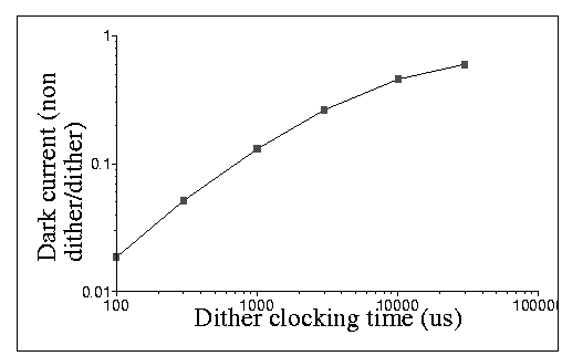
The relative dark signal is plotted as a fraction of the dark current measured with dither clocking against the baseline value found without dither clocking. All measurements were taken at +20 degrees C.
Example, the choice of CCD for Solar-B EIS: MPP or non-MPP ?
Initially, a choice of a Marconi 42-20 non-MPP device was made (termed non-IMO by Marconi). However, it was realised that, given the combination of potential integration times and CCD operating temperature, there was a risk of charge pumping occurring during the latter stages of the mission.
If a trap exists at the boundary between two 'pixels' then each time charge is transferred onto a phase near this trap, an electron may be trapped. This electron may be re-emitted into the same pixel, or it may be re-emitted into the adjacent pixel. Thus, for every dither, it is possible to reduce the charge in one pixel, whilst increasing it in the other. This problem is known as charge pumping and should not be a problem for room temperature testing (as there should be few traps) or at low temperatures (as only one or two dithers will be required).
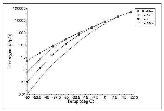
At the end of mission an increased number of traps would be expected (due to proton-induced radiation damage). If the CCD is required to run relatively warmly, then a significant number of dithers may be required to ensure MPP-like operation . The number of dithers required to a set temperature is shown below. For example, if a radiator temperature of -60°C could be achieved then a dither period of about once per second (T=1s) would be sufficient. However, if a temperature of only -55°C could be achieved, then a dither period of ten per second (T=100ms) is required, and so on. Unfortunately, the production of black/white pairs is non-linear, and there appears to be a cut off of about 1000 total dithers, after which noticeable reduction in image quality will occur.
A maximum integration time of 100 seconds was assumed, limiting the
potential number of dithers to no more than 100ms. Due to the problems
of passively cooling the CCD (with a radiator) in a Near Earth Orbit, there
was a risk that the final operating temperature may be too warm to achieve
a reasonable dark current given the maximum possible dither rate. Consequently,
it was decided to use an MPP device (the 42-20 AIMO) for the Solar-B EIS
camera.
Prepared by Chris McFee