| The Basics | How is a CCD clocked out ? | How the charge is measured | Some aspects of CCD behaviour | Why are scientific CCDs so expensive ? |
A Charge Coupled Device (CCD) is a highly sensitive photon detector. The CCD is divided up into a large number of light-sensitive small areas (known as pixels) which can be used to build up an image of the scene of interest. A photon of light which falls within the area defined by one of the pixels will be converted into one (or more) electrons and the number of electrons collected will be directly proportional to the intensity of the scene at each pixel. When the CCD is clocked out, the number of electrons in each pixel are measured and the scene can be reconstructed.
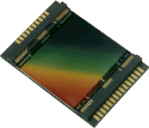
The picture here shows a "typical" CCD. The CCD itself is primarily made of silicon and the structure has been altered so that some of the silicon atoms have been replaced with impurity atoms.
The figure below shows a very simplified cross section through a CCD.
It can be seen that the Silicon itself is not arranged to form individual
pixels. In fact, the pixels are defined by the position of electrodes
above the CCD itself. If a positive voltage is applied to the electrode,
then this positive potential will attract all of the negatively charged
electrons close to the area under the electrode. In addition, any positively
charged holes will be repulsed from the area around the electrode. Consequently
a "potential well" will form in which all the electrons produced by incoming
photons will be stored.
As more and more light falls onto the CCD, then the potential well surrounding
this electrode will attract more and more electrons until the potential
well is full (the amount of electrons that can be stored under a pixel
is known as the full well capacity). To prevent this happening the light
must be prevented from falling onto the CCD for example, by using a shutter
as in a camera. Thus, an image can be made of an object by opening the
shutter, "integrating" for a length of time to fill up most of the electrons
in the potential well, and then closing the shutter to ensure that the
full well capacity is not exceeded.
An actual CCD will consist of a large number of pixels (i.e, potential wells), arranged horizontally in rows and vertically in columns. The number of rows and columns defines the CCD size, typical sizes are 1024 pixels high by 1024 pixels wide. The resolution of the CCD is defined by the size of the pixels, also by their separation (the pixel pitch). In most astronomical CCDs the pixels are touching each other and so the CCD resolution will be defined by the pixel size, typically 10-20µm. Thus, a 1024x1024 sized CCD would have a physical area image size of about 10mm x 10mm.
![]()
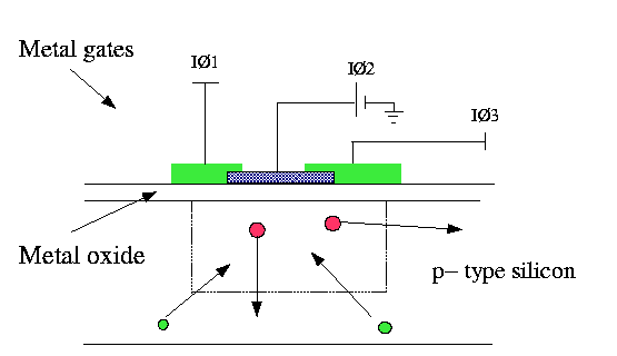
The figure below shows a cross section through a row of a CCD. Each pixel actually consists of three electrodes IØ1, IØ2, and IØ3. Only one of these electrodes is required to create the potential well, but other electrodes are required to transfer the charge out of the CCD. The upper section of the figure (section 1) shows charge being collected under one of the electrodes. To transfer the charge out of the CCD, a new potential well can be created by holding IØ3 high, the charge is now shared between IØ2 and IØ3 (section 2). If IØ2 is now taken low, the charge will be fully transferred under electrode IØ3 (section 3). To continue clocking out the CCD, taking IØ1 high and then taking IØ3 low will ensure that the charge cloud now drifts across under the IØ1 electrodes. As this process is continued, the charge cloud will progress either down the column, or across the row, depending upon the orientation of the electrodes.
![]()
The figure below (called a clocking diagram) shows the progression under which each electrode is held high and low to ensure that charge is transferred through the CCD.
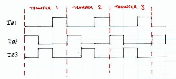
Initially, IØ2 is high - usually to around 12V, and the charge is held under that electrode as in (1) previously. When IØ3 is held high, and IØ2 is taken low (usually 0 V), the charge migrates under the IØ3 electrode (as in (2)). Finally, taking IØ1 high and IØ3 low transfers the charge under IØ1 (as in (3)). This process is repeated in transfer 2 and transfer 3, the charge has now been moved three pixels along. This process is known as charge coupling (hence CCD).
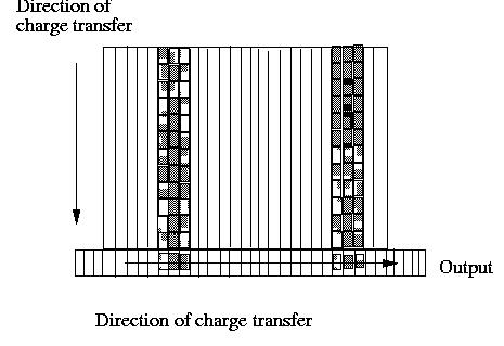
For most of the CCD, the electrodes in each pixel are arranged so that the charge is transferred downwards along the columns. Hence, during the CCD clocking operation, rows are transferred downwards to the final row (the readout register) which is used to transfer the charge in each pixel out of the CCD so it can be measured.
In the read out register, the electrodes are arranged so that the charge
is transferred in the horizontal direction, along the readout register.
The final process on the CCD is the reading of each pixel so that the size of the associated charge cloud can be measured. At the end of the readout register is an amplifier which measure the value of each charge cloud and converts it into a voltage, a typical conversion factor being around 5-10µV per electron with "typical" full well values being about 100,000 electrons or so.
A CCD camera will consist of the CCD chip, and associated electronics,
which is used at this point to amplify the small voltage on the CCD, remove
noise components, digitise the pixel values and output the values of each
pixel for example, to a PC, where the image can be processed in software
and the image displayed. The CCD is an analogue device, and the analogue
voltage values are converted into a digital form by the camera electronics.
Quantum Efficiency
Not every photon falling onto a detector will actually be detected and
converted into an electrical impulse. The percentage of photons that are
actually detected is known as the Quantum Efficiency (QE). For example,
the human eye only has a QE of about 20%, photographic film has a QE of
around 10%, and the best CCDs can achieve a QE of over 80%. Quantum efficiency
will vary with wavelength.
Wavelength range
CCDs can have a wide wavelength range ranging
from about 400nm (blue) to about 1050nm (Infra-red) with a peak sensitivity
at around 700nm. However, using a process known as backthinning, it is
possible to extend the wavelength range of a CCD down into shorter wavelengths
such as the Extreme Ultraviolet and X-ray.
Dynamic Range
The ability to view bright and faint sources correctly in the same image is a very useful property of a detector. The difference between a brightest possible source and the faintest possible source that the detector can accurately see in the same image is known as the dynamic range. When light falls onto a CCD the photons are converted into electrons. Consequently, the dynamic range of a CCD is usually discussed in terms of the minimum and maximum number of electrons that can be imaged. As more light falls onto the CCD, more and more electrons are collected in a potential well, and eventually no more electrons can be accommodated within the potential well and the pixel is said to be saturated. For a typical scientific CCD this may occur at around 150,000 electrons or so. The minimum signal that can be detected is not necessarily one electron (corresponding to one photon at visible wavelengths). In fact, there is a minimum amount of electronic noise which is associated with the physical structure of the CCD and is usually around 2-4 electrons for each pixel. Thus, the minimum signal that can be detected is determined by this readout noise.
In the example above, the CCD would have a dynamic range of 150,000:4 (taking the upper noise level). But - this dynamic range is also dependent on the ability of the electronics to be able fully digitise all of this dynamic range (see the more detailed CCD information for discussions on electronics resolution).
Linearity
On the whole, the eye is not a linear detector (except over very small
variations in intensity) and has a logarithmic response. An important consideration
in a detector is its ability to respond linearly to any image it views.
By this we mean that if it detects 100 photons it will convert these to
100 electrons (if we had 100% QE) and if it detects 10000 photons, it will
convert these to 10000 electrons. In such a situation, we say that the
detector has a linear response. Such a response is obviously very useful
as there is no need for any additional processing on the image to determine
the 'true' intensity of different objects in an image.
Noise
One of the most important aspects of CCD performance is its noise response. There are a number of contributions to the noise performance of a CCD, these are briefly listed here:
Power
CCDs themselves consume very little power. During
integration, only a very small current is flowing and the CCD consumes
only 50mW or so. Whilst the CCD is being clocked out more power can be
consumed but this is typically only several Watts or so. Of course, the
electronics required to operate the CCD and process images can consume
much more power.
Why are scientific CCDs so
expensive ?
A Video camera using a CCD can be bought for as little as 400-500 pounds.
However, a scientific grade CCD may cost up to 100 times this price, sometimes
more. Some of the reasons why scientific CCDs are much more expensive than
CCDs in consumer electronics are outlined below:
Cost and complexity
Scientific grade CCDs are much more expensive than the basic type of CCDs that are usually found in devices such as commercially available Video cameras. Commercially available video cameras normally have a number of disadvantages that make them unsuitable for scientific use. For example:
Prepared by Chris McFee