A short note summarising the potential CCD operating temperature
Technical note: MSSL/SLB-EIS/TN/05
Author : Chris McFee, 15/2/2000
1 Introduction
I have produced several design notes trying to determine the optimum operating temperature of the CCD (along with the optimum shielding depth, which is a related issue)1. This short memo summarises my assessment of the optimum temperature.
The CCD temperature will be mostly determined by three major issues which could degrade the CCD imaging quality:
· dark signal;
· hot pixels;
· charge transfer inefficiency (CTI).
It has also become clear that the potential CCD temperature could also affect the choice of device (i.e., MPP or non-MPP).
These issues are discussed below.
2 Dark signal
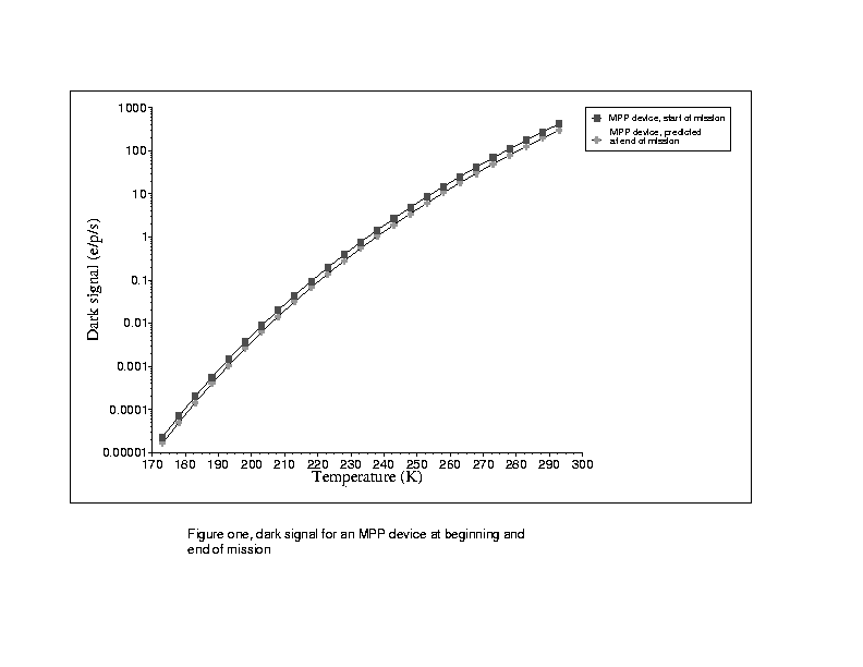
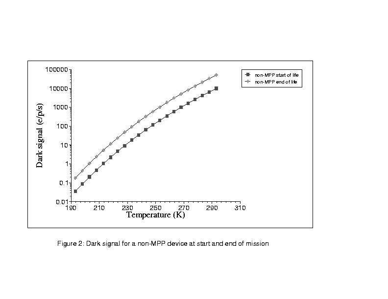
The dark signal of the 42-10 can be accurately predicted, both at the start of the mission, and after a (nominal) five year radiation dose. We have a choice whether we select an MPP or a non-MPP device. Marconi recommend a non-MPP device to maximise the full well, but we will have to implement dither clocking to reduce the dark current for the non-MPP device. Figures one and two below show predicted values for both MPP and non-MPP devices and a short summary of the advantages and disadvantages of each device is also described below.
MPP devices
advantages
· better dark current characteristics without requiring dither clocking;
· hence, easier electronics;
· marginally better radiation tolerance;
disadvantages
· lower full well capacity ~90k electrons compared with ~120k for non-MPP;
· slightly lower clocking speeds are possible;
· no supplementary buried channel is possible (due to difficulty for Marconi of producing both MPP implant and supplementary buried channel) - hence likely to have higher CTI
Non-MPP devices
advantages
· larger full well;
disadvantages
· some higher complexity required to implement 'dither clocking' to reduce dark current to MPP levels;
· potential for 'charge pumping' producing black/white pairs (see later for a discussion on charge pumping).
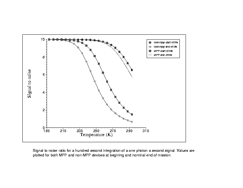
Expected dark current levels for MPP and non-MPP, at the start and at the end of the mission, are shown in figures one and two. One key parameter related to the CCD dark current is the signal to noise ratio that will be obtained for weak signals. Figure three shows the signal to noise ratio calculated for a signal of one photon/pixel/s, integrated for 100 seconds.
The three sources of noise that have been considered are:
· the shot noise on the signal;
· the rms readout noise - assumed to be 8 electrons per pixel;
· the dark current.
Data is plotted for an MPP device, using values of dark current calculated at the start and the end of the mission; and for a non-MPP device, again using values of dark current calculated at the start and the end of the mission. It can be seen that a non-MPP device requires a significantly lower operating temperature to achieve a signal to noise approaching 10 for a quite Sun region. Expressing in terms of dark current, we would probably wish to achieve no more than 0.1 electrons/pixel/s and could not live with any more than 1 electron/pixel/s. Assuming MPP-like operation, this leads to a preferred operating temperature at end of mission of about -53°C, with an absolute limit of operating temperature of -35°C.
A technique known as dither clocking (also known as "charge sloshing") can be used to reduce the dark signal to approaching that of an MPP device - this technique is used in XMM-EPIC. As the full well capacity of a non-MPP device is higher, then using a dithered non-MPP device is obviously preferred. Consequently, in most circumstances, the use of a non-MPP CCD is advised by Marconi. Room temperature operation is possible using a dither rate of around 50µs and MPP-like dark current can be achieved at low temperatures using just several dithers during an integration.
Thus, it initially appears that a non-MPP device should be used. However, there is an additional problem of "charge pumping" which could reduce the image quality later on in the mission. To remove this problem, a reduced dither rate would have to be used which would limit the dark current (and hence signal to noise that could be achieved). This is explained below.
The problem of 'charge pumping' for warmer CCD temperatures
If a trap exists at the boundary between two 'pixels' then each time charge is transferred onto a phase near this trap, an electron may be trapped. This electron may be re-emitted into the same pixel, or it may be re-emitted into the adjacent pixel. Thus, for every dither, it is possible to reduce the charge in one pixel, whilst increasing it in the other. This problem is known as charge pumping and should not be a problem for room temperature testing (as there should be few traps) or at low temperatures (as only one or two dithers will be required).
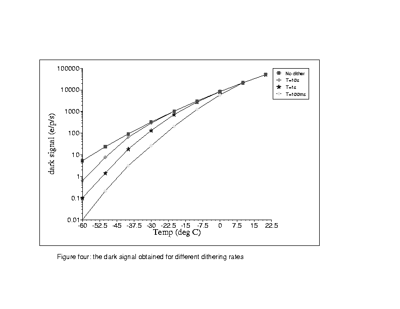
However, at the end of mission an increased number of traps would be expected (due to proton-induced radiation damage). If the CCD is required to run relatively warmly, then a significant number of dithers may be required to ensure MPP-like operation to achieve the dark currents discussed above. The number of dithers required to a set temperature is shown in figure four. For example, if a radiator temperature of -60°C could be achieved then a dither period of about once per second (T=1s) would be sufficient. However, if a temperature of only -55°C could be achieved, then a dither period of ten per second (T=100ms) is required, and so on.
Unfortunately, the production of black/white pairs is non-linear, and there appears to be a cut off of about 1000 total dithers, after which noticeable reduction in image quality will occur. We are thus limited to a dither period of no more than 100ms, assuming that the maximum quite Sun integration time is no more than 100s. Using the dark current figures discussed above, ideally we will need a radiator temperature of no less than -52°C at the end of mission. Certainly, we can tolerate no more than -48°C at the end of mission if we are to use an non-MPP device.
3 'Hot' pixels
The distribution of hot pixels will depend on the yield from the CCD
batch. The specification from Marconi is given below for -60°C. It
may
be worse at -50°C but it is not possible to predict the degradation
in a simple way and it is unlikely that the distribution of hot pixels
will differ significantly from the -60°C figures.
| Black spots | 40 | Have a responsivity of less than 80% of the local mean signal. |
| White spots | 20 | Have a generation rate equivalent to 100 electrons per pixel per hour at 153K. |
| Traps | 2 | A capacity greater than 200 electrons at 153K. |
4 Charge transfer inefficiency (CTI)
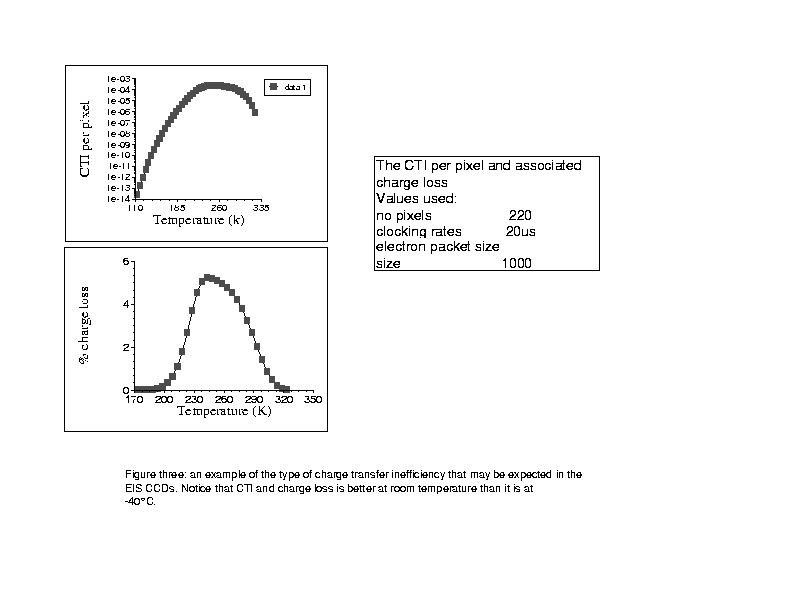
Possible charge transfer effects have been discussed in some detail in a number of Solar-B EIS design notes. In general, CTI is related to a range of parameters, for example: signal size (including dark current); clocking time; and radiation dose (related to radiation damage). Consequently, as for the distribution of hot pixels, it is not possible to definitively predict the changes in CTI . However, the CTI problem is likely to diminish as the temperature decreases because the trapping time constants will become longer and will begin to exceed the time taken to transfer a line of charge through the serial register. For example, at -60°C the emission time constant for a PV centre (thought to be the dominant traping centre at these temperatures) is around 20ms (reference 2) which means that, at typical line transfer time of 2ms, few traps would become available during a transfer during the serial register for any particular CCD row. Nevertheless, some trapping would still occur as it will take about 1s to completely clock out all rows on a 42-10 (a temperature of about -100°C is required for a time constant of ~1s).
A speadsheet type model can be used to try and estimate the potential loss of charge transfer efficiency (for example, see Hardy [3]). Using such a spreadsheet, Figure 5 shows the variation for the radiation dose of 3x10⁹ protons/cm2 which should occur with the preferred shielding of 15mm Al equivalent. A ten degree drop in temperature should reduce the CTI by about a factor of three. However, it must be emphasised that the calculation is very simplistic and should best be used just to give an indication of the way in which CTI can be reduced by lowering the temperature. Similar results can be obtained simply by seeing how the PV centre trap time constant increases with lower temperature.
5 Summary
The derivation of the optimum operating temperature has to be a judgement
and cannot be quantitatively predicted. Consequently, I have produced a
table summarising my 'best judgement' on each of the four issues discussed
above.
| Operating temp | -40°C | -60°C | -80°C |
| Dark current | ok | ok | ok |
| Hot pixels | ? | should be ok | ok |
| CTI | ? | ? | should be ok |
| MPP/non-MPP | MPP | non-MPP | non-MPP |
Thus, my judgment is for an optimal CCD operating temperature of
-80°C to minimise the CTI and to enable the purchase of a non-MPP
device (which is I think is a better device). However, this is basically
a judgement, partly based (as well as the above analysis) both on the sort
of temperatures similar missions have adopted and from analysis of relevant
CTI literature. For example, if CTI is not a problem (which it may not
be as some conservative assumptions have been made) then a much lower operating
temperature can be chosen, depending on factors such as the dark current
required. If the driver is to use a non-MPP device then a temperature
around -60°C /-50°C should be aimed for. Below that, an MPP device
may be required.
6 Referenced documents
[1] CCD radiation damage study. G. R. Hopkinson . Sira contract A/9503/00. April 1995
[2] I. H Bond - Radiation Damage in Optical Charge Coupled Devices , PhD thesis 1996, UCL
[3] Hardy, T. - Charge Transfer Efficiency in Proton Damaged CCDs. IEEE Transactions on Nuclear Science, vol 45 (2), pp 154-163. 1998