|
|
|
|
Types of noise in a CCD
When a CCD image is taken, noise will appear as well as the main CCD image. Noise can be thought of as unwanted signal which doesn't improve the quality of the image. In fact, it will degrade it. The main problem with noise is that most noise is essentially random, and so cannot be completely removed from the image. For example, if we know that a noise source contributes 10 units on each image we can subtract those 10 units from the image. If we only know that the noise is 'around' 10 units, then we can't completely remove all of this noise (as we don't know its exact value).
The main contributions to CCD noise are:
Noise on the image itself ("shot noise")
The detection of photons by the CCD is a statistical process. If images
are taken over several (equal) time periods, then the intensity (the number
of photons recorded) will not be the same for each image but will vary
slightly. If enough images are taken, it will be seen that the deviation
in intensity found for each image follows the well known Poisson distribution.
In effect, we cannot be sure that the intensity we have measured in a particular
image represents the "true" intensity as we know that this value will deviate
from the average. It is this deviation which is considered to be the noise
associated with the image. As the deviation is known to follow a Poisson
distribution, we know that the likely deviation will be plus or minus the
square root of the signal intensity measured. Thus, if we measure a signal
intensity of one hundred photons, then the noise on this signal will be
ten photons. If we measure a signal intensity of one thousand photons in
the image, then the noise on this signal will be about thirty one photons.
Thermally generated noise:
Additional electrons will be generated within the CCD not by the absorption
of photons (i.e the signal) but by physical processes within the CCD itself.
The number of electrons generated in a second will be dependent on the
operating temperature of the CCD and hence this noise is known as thermal
noise (sometimes also known as dark noise). As with the detection
of the signal, the same number of electrons will not be generated in equivalent
periods of time as the thermal noise will also have a Poisson distribution.
Other noise contributions also affect image quality. A very good description of how noise can affect the quality of CCD images can be found on the Sky and Telescope CCD imaging pages.
Some of the Physics behind the generation of various types of noise
within a CCD are explained below.
Some Physical Principles behind CCD noise
Even in the absence of light, thermally generated electrons will be collected in the CCD and will contribute to the overall signal measured. There are three main contributions to dark current:
However, if the interface states are filled up by free carriers then the dark current will be drastically reduced. Such a process can be achieved by operating the CCD in inversion which is a technique used by all modern CCDs. When the CCD is operated in inverted mode, holes from the channel stops migrate to fill the interface states. Two of the three electrodes defining a pixel are driven into inversion to drastically reduce the dark current (it is not possible to invert all three electrodes as a potential well is still required to collect charge). If a CCD is not inverted, then the dark current generation rate may be as high as several hundreds of thousands of electrons per pixel per second (at room temperature) whereas an inverted CCD will have a much lower generation rate of about ten thousand electrons per pixel per second.
If such a CCD is read out a number of times per second (for example in a video camera) then the dark current at room temperature is low enough not to significantly interfere with image quality. However, if the CCD is only read out once a second (or less frequently) then the number of thermally generated electrons will be to high for adequate image quality. Hence, additional measures need to be taken.
The simplest way to reduce the dark current is to cool the CCD as dark
current generation is temperature related.
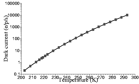
The figure below shows the variation in dark current with temperature
for a CCD with a room temperature dark current of 10,000 electrons/pixel/s.
There are a number of ways in which a CCD can be cooled, the easiest is
to use liquid Nitrogen but thermoelectric coolers (Peltier coolers) can
be used, and in space the CCD can be cooled with a direct connection to
a passive radiator.
A second way of reducing the dark noise in a CCD is to use a Multi-Pinned Phase (MPP) device. In an MPP device, it is possible to operate the CCD with all three electrode phases driven into inversion. This is accomplished by adding a suitable dopant under one of the phases during CCD fabrication. The presence of the additional dopant under one of the phases alters the potential under that phase so that there is still a potential well present during integration when all the electrode phases are at clock low level (usually zero volts). Dark current is now only generated in the bulk silicon reducing the dark current to about 300 electrons/pixel/signal.
The ultimate noise limit of the CCD is determined by the readout noise.
The readout noise is the noise of the on-chip amplifier which converts
the charge (i.e the electrons) into a change in analogue voltage using:
Q= CV where Q is the charge on the output node, and C is the output
node capacitance. V is the voltage sensed by the on-chip amplifier operating
as a source follower.
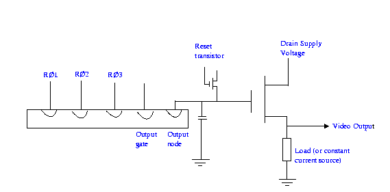
The figure above shows a schematic of a typical CCD output section.
The charge in a pixel is transferred onto the output node where the change
in voltage caused by this charge is sensed by the on-chip amplifier.
The on-chip amplifier will have an associated noise performance which
is typically 1/f at low sampling frequencies with a white noise floor at
higher sampling frequencies. The sampling frequency corresponds to the
rate at which each pixel is read by the CCD.
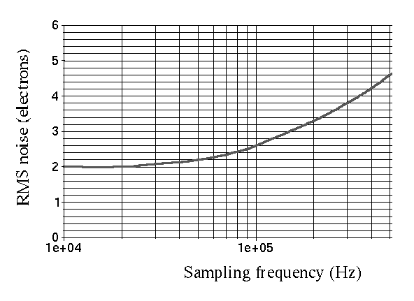
The figure above shows the readout noise response versus the sampling frequency for a typical CCD. It can be seen that as the sampling frequency increases, the root mean square value of the read out noise increases.
Prepared by Chris McFee