MHC Power Board, development model two.
This page is not intended as an official document and is only to be used as a guide to the performance of this unit at this time.
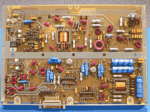
Full resolution image of MHC Power Board.
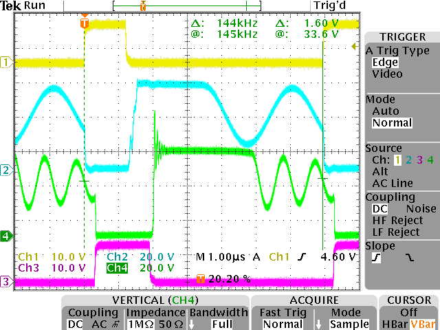
Here are plots showing the performance of the pcb at this time, 07/05/02.
Converter A supplies the +120V, +/-15VA and +/-5VA for the analogue electronics.
Converter B supplies the digital +5VD and +15VM for the mechanisms.
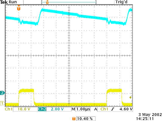
Converter primary waveforms.
Plot 00: Converters running in phase at 144KHz with maximum loads
(Max loads are +5VD 390mA, +15VM 234mA (not on on power up) +120V 1mA, +/-15VA 65mA, +5VA 13mA, -5VA 24mA)
Ch1 Yellow, Converter A FET Gate
Ch2 Blue , Converter A FET Drain
Ch3 Pink , Converter B FET Gate
Ch4 Green , Converter B FET Drain
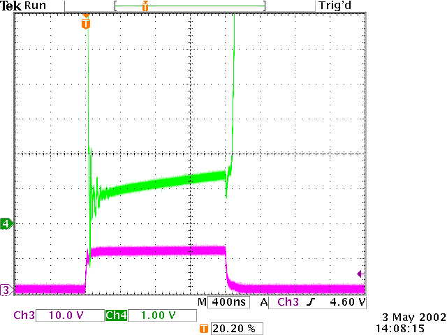
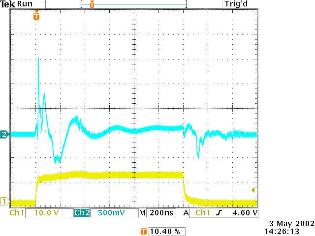
Converter B primary waveforms.
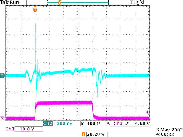
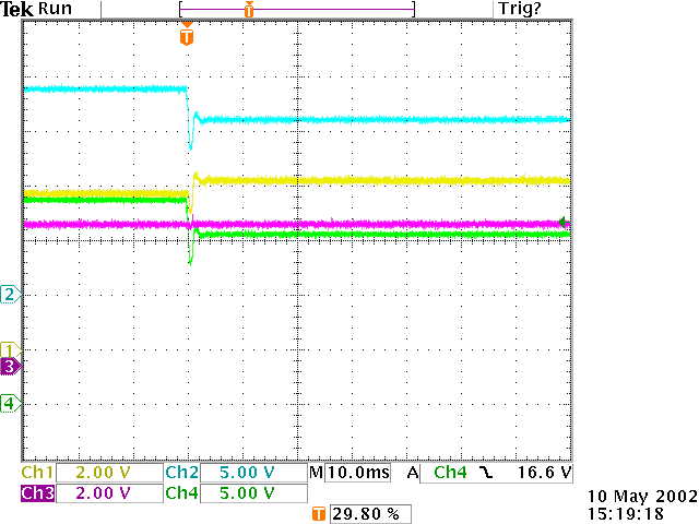
Plot 01 and 02: Looking at the current through the primary of converter B using a 0.1R resistor in the Source of the FET, max load.
Ch1 Yellow,
Ch2 Blue , Converter B FET Source
Ch3 Pink , Converter B FET Gate
Ch4 Green ,
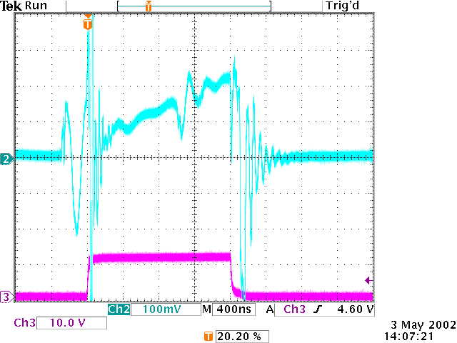
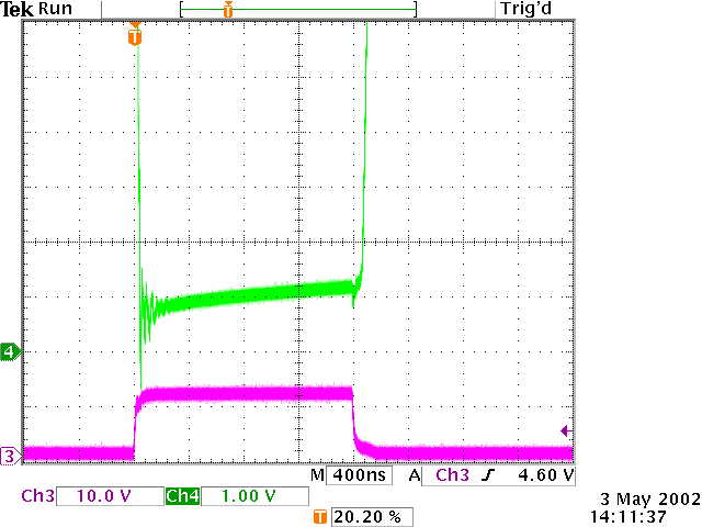
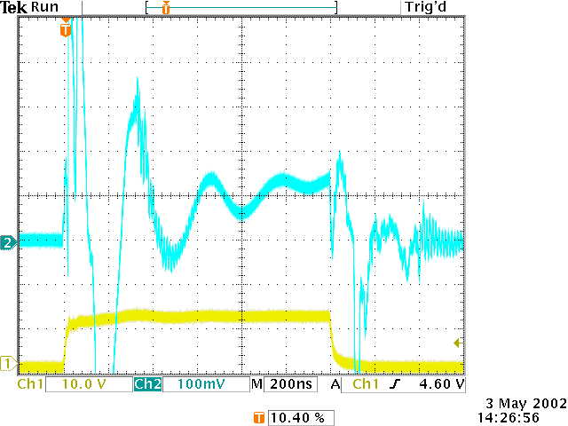
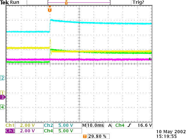
Plot 03: Checking the voltage drop across the Converter B FET when switched on, 0.1R still in Source.
Ch1 Yellow,
Ch2 Blue ,
Ch3 Pink , Converter B FET Gate
Ch4 Green , B Drain
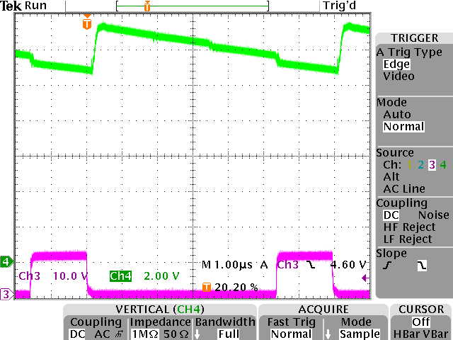
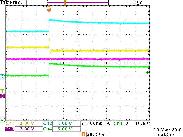
Plot 04: Same as Plot 03 but with the 0.1R removed.
Plot 05: Looking at the ripple on the Vaux line. This is the transformer feedback and power for the PWM chip. The amount of filtering on this line has been reduced to a minimal level to maintain the stability of the converters, hence the sawtooth waveform. The filtering on all other secondary voltages remains and gives a very low ripple which can be seen in later plots.
Ch1 Yellow,
Ch2 Blue ,
Ch3 Pink , Converter B FET Gate
Ch4 Green , B Vaux
Converter A primary waveforms.
Plot 06: Max load.
Ch1 Yellow, A Gate
Ch2 Blue , A Drain
Ch3 Pink ,
Ch4 Green ,
Plot 07: Max load.
Ch1 Yellow, A Gate
Ch2 Blue , A Vaux
Ch3 Pink ,
Ch4 Green ,
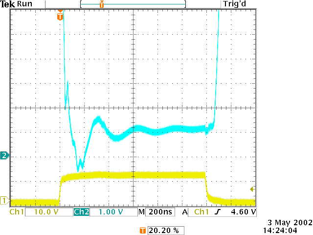
Plot 08 and 09: Looking at the current through the primary using a 0.1R resistor in the Source.
Ch1 Yellow, A Gate
Ch2 Blue , A Source
Ch3 Pink ,
Ch4 Green ,
Converter B secondary waveforms.
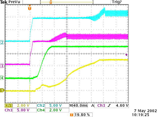
Plot 10: Turn on of converter B, showing the relationship of Vaux and the +5VD regulator ouput. The load on the +5V line is 390mA. The +5V regulator current limit is set between 500 and 550mA. Once the current limit is reached the ouput voltage starts to droop.
Note that the +15VM current limit circuit will not allow any power dissipation on power up. Any load will have to be removed and then re-applied before current is allowed to flow. The current limit is set to about 450mA at this time and can be adjusted by changing the value of one resistor. Once the limit has 'fired' the converter power (hence the whole of the MHC) will have to be cycled bofore it can be used again.
Ch1 Yellow,
Ch2 Blue , B Vaux
Ch3 Pink ,
Ch4 Green , +5VD regulator output.
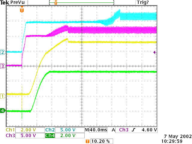
Plot 11: Same as Plot 10 except the +5VD winding output is also shown.
Ch1 Yellow, +5VD winding output.
Ch2 Blue , B Vaux
Ch3 Pink ,
Ch4 Green , +5VD regulator output.
Plot 12: Same as Plot 11 except the +5VD load is 150mA not 390mA.
Ch1 Yellow, +5VD winding output.
Ch2 Blue , B Vaux
Ch3 Pink ,
Ch4 Green , +5VD regulator output.
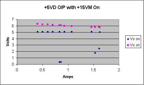
Plot 13: Same as Plot 11 except the +15VM winding output is also shown. The +15VM output is not regulated and varies from 18.7V with no load, to 15.5V with a load of 234mA.
Ch1 Yellow, +5VD winding output.
Ch2 Blue , B Vaux
Ch3 Pink , +15VM winding output.
Ch4 Green , +5VD regulator output.
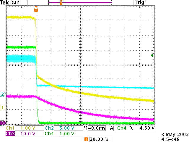
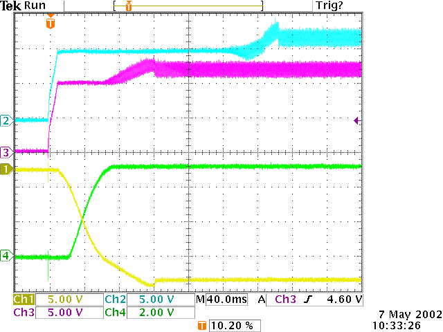
Plot 14: Turn off from +5VD at 390mA and +15VM at 0mA.
Ch1 Yellow, +5VD winding output.
Ch2 Blue , B Vaux
Ch3 Pink , +15VM winding output.
Ch4 Green , +5VD regulator output.

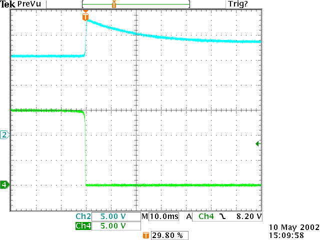
Plot 15: Turn off from +5VD at 150mA and +15VM at 234mA.
Ch1 Yellow, +5VD winding output.
Ch2 Blue , B Vaux
Ch3 Pink , +15VM winding output.
Ch4 Green , +5VD regulator output.
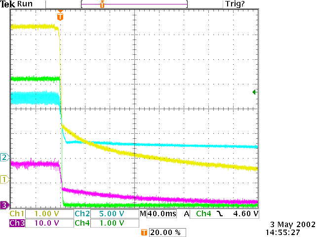
Plot 16: Turn off from +5VD at 390mA and +15VM at 0mA (Same as plot 14).
Ch1 Yellow, +5VD winding output.
Ch2 Blue , B Vaux
Ch3 Pink , +15VM winding output.
Ch4 Green , +5VD regulator output.
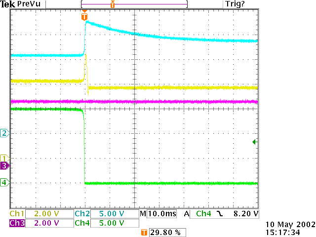
Plot 17: Turn off from +5VD at 390mA and +15VM at 234mA.
Ch1 Yellow, +5VD winding output.
Ch2 Blue , B Vaux
Ch3 Pink , +15VM winding output.
Ch4 Green , +5VD regulator output.
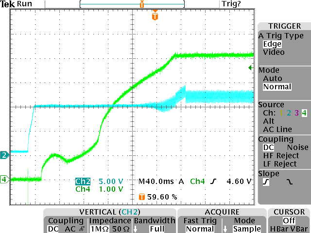
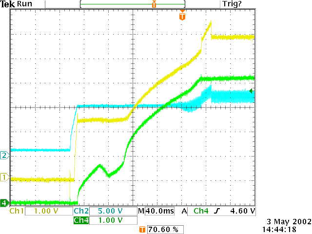
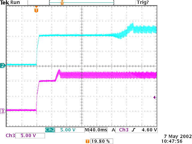
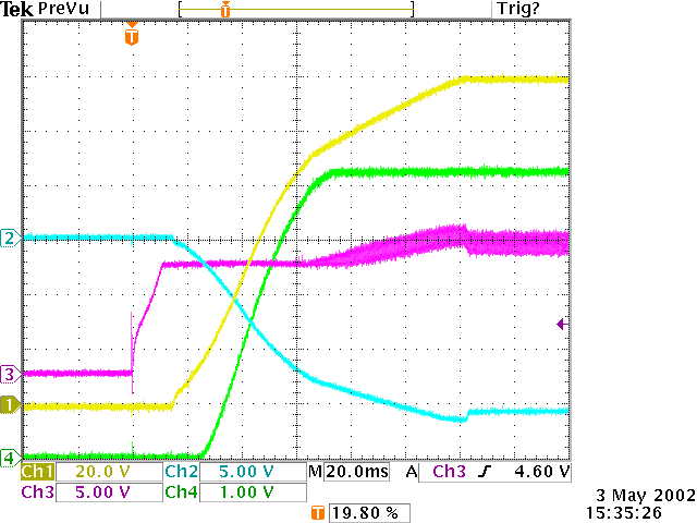
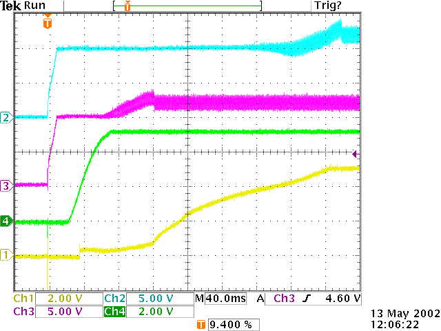
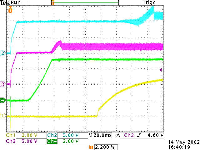
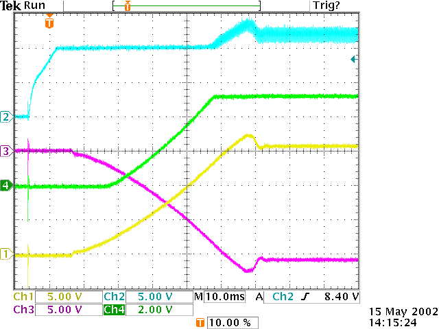
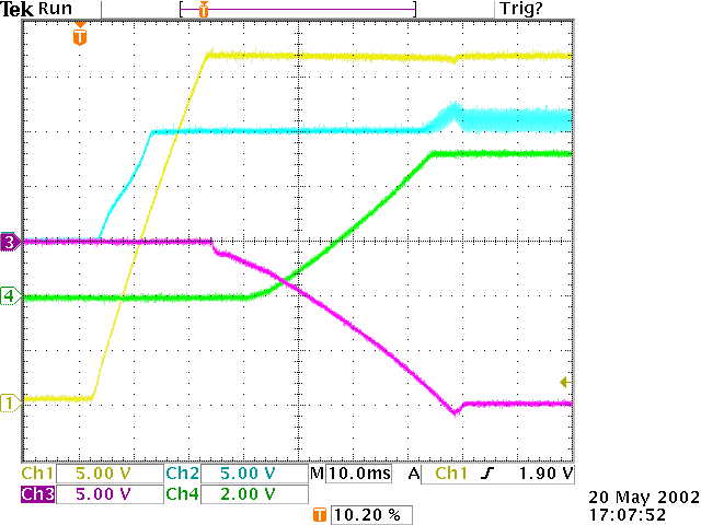
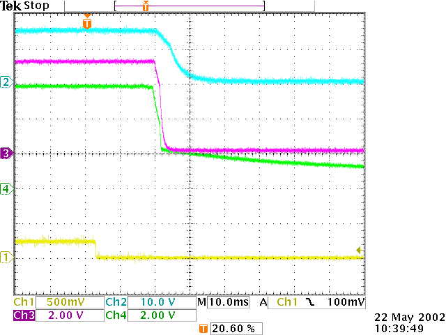
Comparison of converter turn on and off timings.
The Requirement is for the +5VD to come up after the analogue supplies.
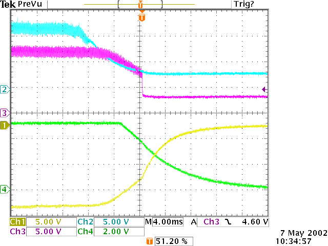
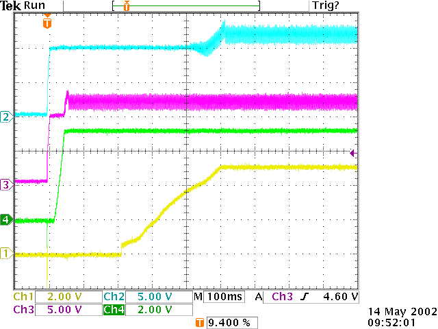
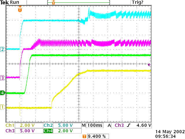
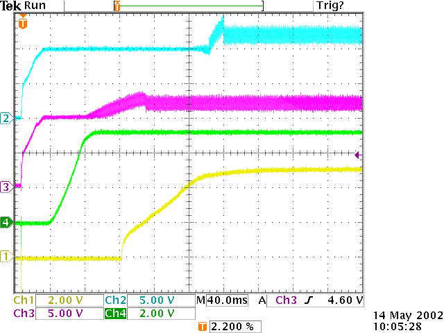
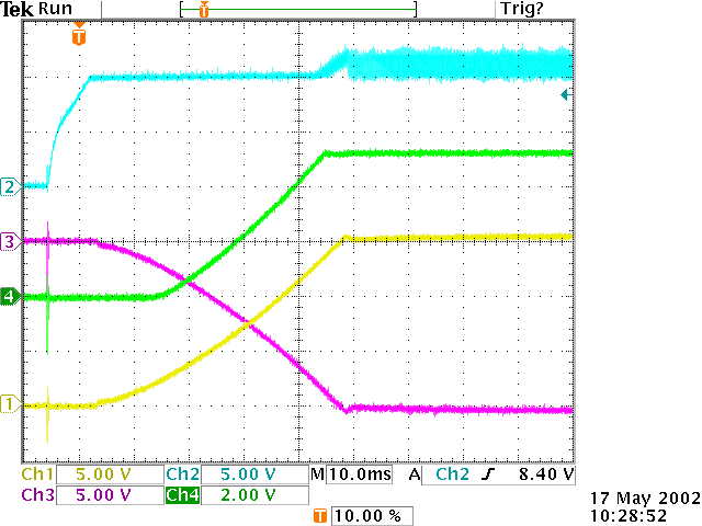
Plot 18: Turn on, both converters at maximum load. Mains power supply limit set to 450mA.
The initial rise shows the startup power to the PWM chips. This is derived from the main input power. The voltage then shows ripple (see plot 5 for explanation) when the Vaux voltage from the transformer rises up above the start up supply. The PWM chip then starts to control the outputs. As can be seen, converter A starts up more quickly than converter B.
Ch1 Yellow,
Ch2 Blue , B Vaux.
Ch3 Pink , A Vaux.
Ch4 Green ,
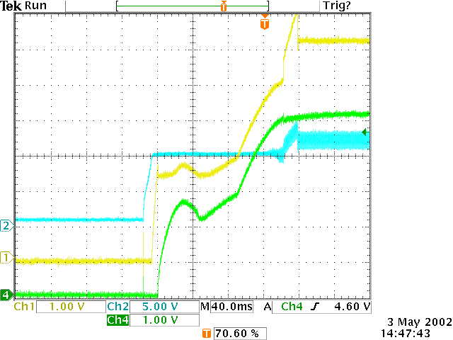
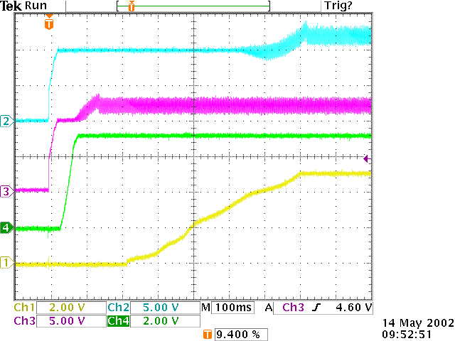
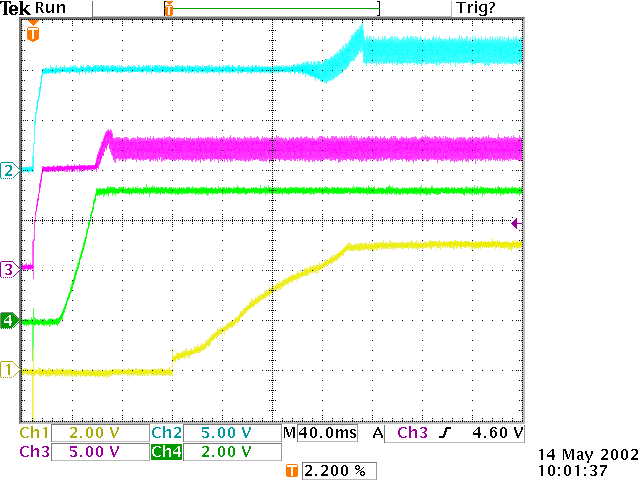
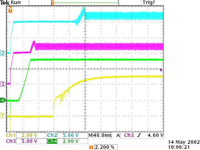
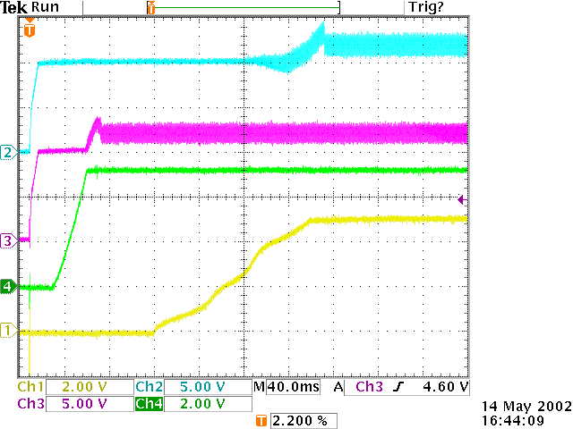
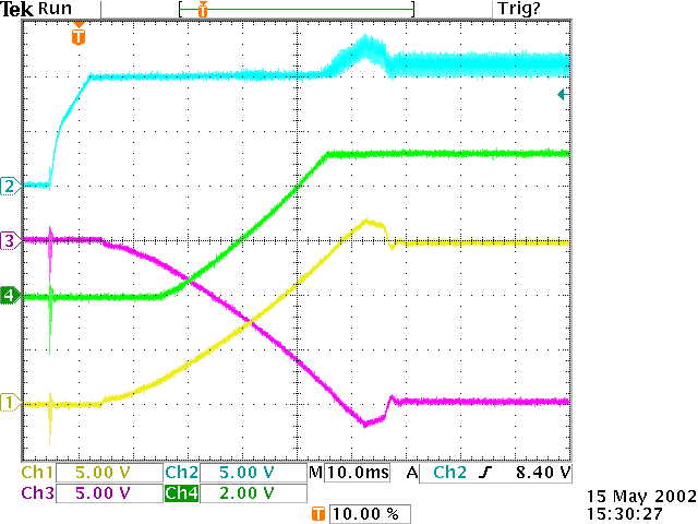
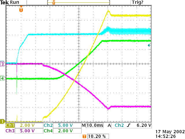
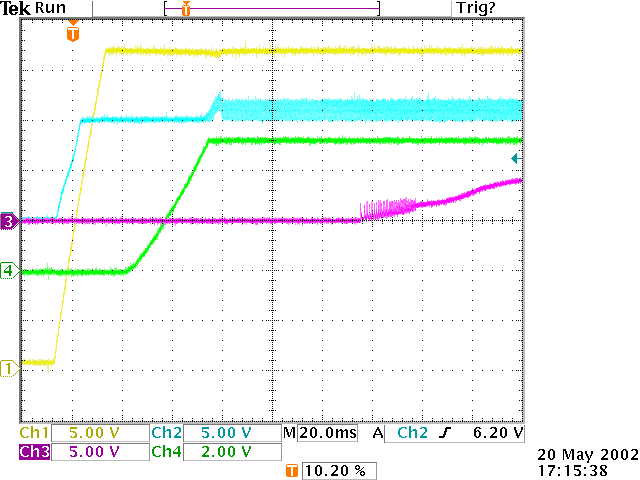
Plot 19: Turn on, Converter A max load and converter B minimum load. Mains power supply limit set to 450mA. Shows Converter B starting up more quickly, but still after converter A.
Ch1 Yellow,
Ch2 Blue , B Vaux.
Ch3 Pink , A Vaux.
Ch4 Green ,
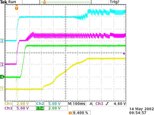
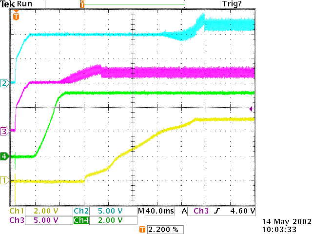
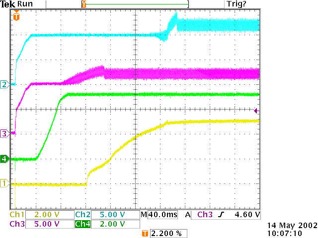
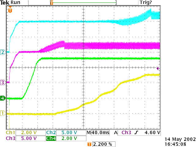
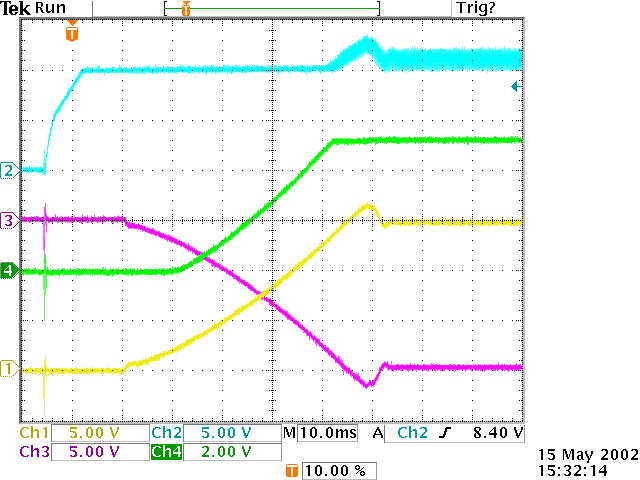
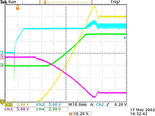
Plot 20: Turn on, both converters at maximum load. Mains power supply limit set to 1100mA. Checking that the mains power pack is not having a great effect on the start up performance.
Ch1 Yellow,
Ch2 Blue , B Vaux.
Ch3 Pink , A Vaux.
Ch4 Green ,
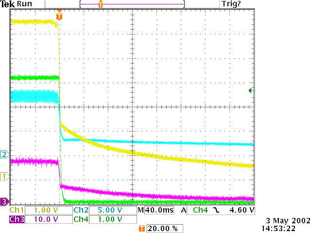
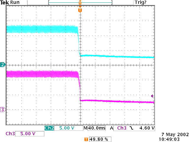
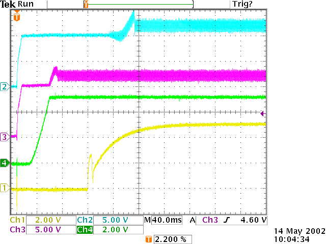
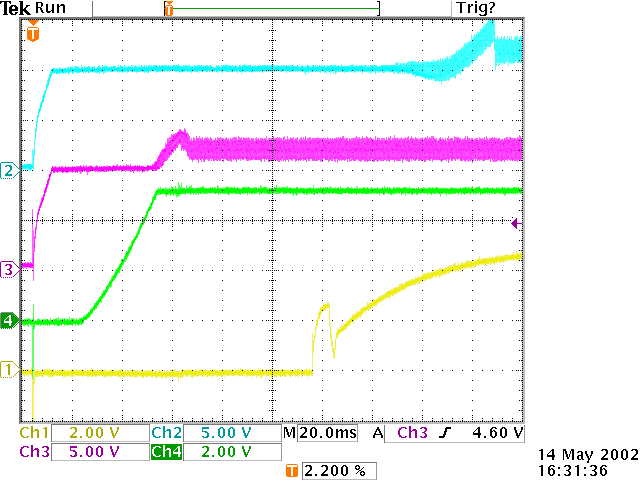
Plot 21: Turn off, both converters at maximum load.
Ch1 Yellow,
Ch2 Blue , B Vaux.
Ch3 Pink , A Vaux.
Ch4 Green ,
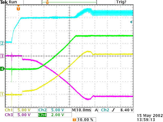
Plot 22: Turn off, both converters at maximum load. Mains power supply limit set to 450mA. Also showing the +5VD and +5VA regulator outputs.
Ch1 Yellow, +5VD regulator output.
Ch2 Blue , B Vaux.
Ch3 Pink , A Vaux.
Ch4 Green , +5VA regulator output.
Plot 23: Same as 22 but different trigger position.
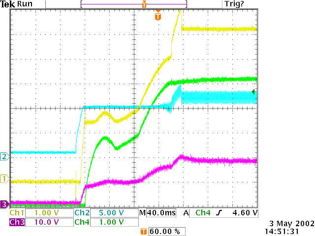
Plot 24: Turn on, both converters at maximum load. Mains power supply limit set to 450mA.
Ch1 Yellow, +5VD regulator output.
Ch2 Blue , B Vaux.
Ch3 Pink , A Vaux.
Ch4 Green , +5VA regulator output.
Plot 25: Turn on, both converters at maximum load. Mains power supply limit set to 450mA. Showing the +5VA winding compared to the regulator output.
Ch1 Yellow, +5VA winding output.
Ch2 Blue , B Vaux.
Ch3 Pink , A Vaux.
Ch4 Green , +5VA regulator output.
Plot 26: Turn on, both converters at maximum load. Mains power supply limit set to 450mA. Also showing the -15VA output. The +/-15VA outputs are not regulated and vary in the range of 15.5 to 16.0V depending on the transformer loading.
Ch1 Yellow, +5VA winding output.
Ch2 Blue , -15VA.
Ch3 Pink , A Vaux.
Ch4 Green , +5VA regulator output.
Plot 27: Turn off, both converters at maximum load. Mains power supply limit set to 450mA.
Ch1 Yellow, +5VA winding output.
Ch2 Blue , -15VA.
Ch3 Pink , A Vaux.
Ch4 Green , +5VA regulator output.
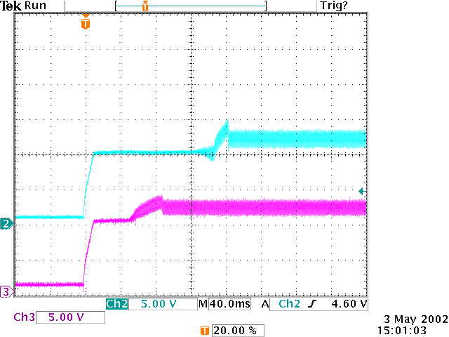
Plot 28: Turn on, both converters at maximum load. Mains power supply limit set to 450mA. Also showing the +120VA output. The +120VA output is not regulated and varies in the range of 120 to 126V depending on the transformer loading.
Ch1 Yellow, +120VA.
Ch2 Blue , -15VA.
Ch3 Pink , A Vaux.
Ch4 Green , +5VA regulator output.
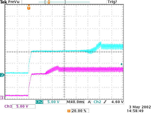
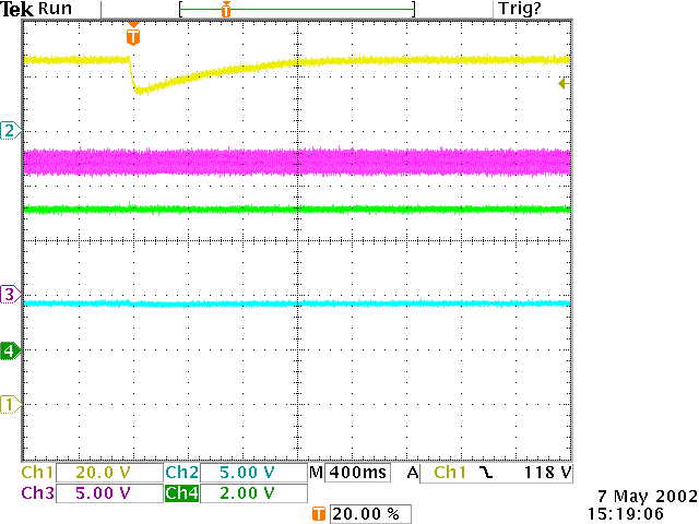
Plot 29: This plot shows the recovery time of the +120VA output to switching in a 100uF load.
Ch1 Yellow, +120VA.
Ch2 Blue , -15VA.
Ch3 Pink , A Vaux.
Ch4 Green , +5VA regulator output.
Checking the behaviour Converter B with different conditions on the +15VM line.
Plot 30: The +15VM current limit firing at 420mA.
Ch1 Yellow,
Ch2 Blue , +15VM winding O/P.
Ch3 Pink ,
Ch4 Green , +15VM current limit O/P.
Plot 31: The +15VM current limit firing at 420mA and the response on the +5VD line.
Ch1 Yellow, +5VD winding O/P.
Ch2 Blue , +15VM winding O/P.
Ch3 Pink , +5VD regulator O/P.
Ch4 Green , +15VM current limit O/P.
Plot 32: A load of 240mA being switched into the +15VM output.
Ch1 Yellow, +5VD winding O/P.
Ch2 Blue , +15VM winding O/P.
Ch3 Pink , +5VD regulator O/P.
Ch4 Green , +15VM current limit O/P.
Plot 33 and 34: Switching off a 240mA load on the +15VM load.
Ch1 Yellow, +5VD winding O/P.
Ch2 Blue , +15VM winding O/P.
Ch3 Pink , +5VD regulator O/P.
Ch4 Green , +15VM current limit O/P.
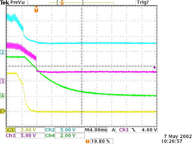
More testing of the start up time of Converter B compared to converter A.
Converter B is set up with different loads and the start up capacitor value is also changed. Different supply voltages are used to simulate the possible worst case values from the spacecraft. Converter A has max loads for all the following maeasurements to give the slowest start up time for +5VA.
Plot 35: Same as plot 25 but +5VD at 700mA. Mains power supply limit set to 450mA at 31V.
Ch1 Yellow, +5VD regulator output.
Ch2 Blue , B Vaux.
Ch3 Pink , A Vaux
Ch4 Green , +5VA regulator output.
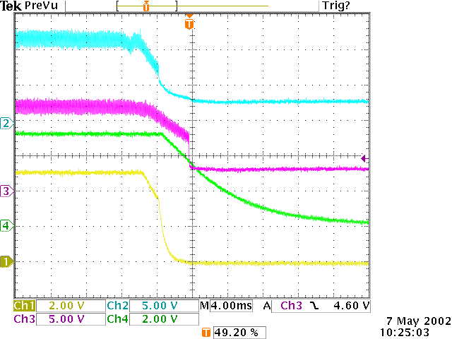
Some of the previous measurements of the relative start up timing may not have given enough time between turn on to let the start up capacitors discharge. This may have meant that the relative times were shorter than they actually are. The following measurements included shorting out the start up capacitor for Converter B which gives a more realistic measurement.
Plot 36: +5VD at 700mA. Mains power supply limit set to 1100mA at 31V.
Ch1 Yellow, +5VD regulator output.
Ch2 Blue , B Vaux.
Ch3 Pink , A Vaux
Ch4 Green , +5VA regulator output.
Plot 37: +5VD at 700mA. Mains power supply 1100mA at 20V. This plot shows the slowest start up time of about 500mS. This could well be too slow so the start up capacitor is reduced and another data set taken, see plots 42-49.
Ch1 Yellow, +5VD regulator output.
Ch2 Blue , B Vaux.
Ch3 Pink , A Vaux
Ch4 Green , +5VA regulator output.
Plot 38: +5VD at 390mA. Mains power supply 1100mA at 31V.
Ch1 Yellow, +5VD regulator output.
Ch2 Blue , B Vaux.
Ch3 Pink , A Vaux
Ch4 Green , +5VA regulator output.

Plot 39: +5VD at 390mA. Mains power supply 1100mA at 20V. (The effect seen on the Vaux lines is aliasing between the Vaux ripple and the digital scope sampling and is not a real effect.)
Ch1 Yellow, +5VD regulator output.
Ch2 Blue , B Vaux.
Ch3 Pink , A Vaux
Ch4 Green , +5VA regulator output.
Plot 40: +5VD at 150mA. Mains power supply 1100mA at 31V. The start profile of the +5VD regulator shows a glitch in this case with low load. This can also be seen in some subsequent plots with similar test conditions. There is a modification which will remove this.
Ch1 Yellow, +5VD regulator output.
Ch2 Blue , B Vaux.
Ch3 Pink , A Vaux
Ch4 Green , +5VA regulator output.
Plot 41: +5VD at 150mA. Mains power supply 1100mA at 20V.
Ch1 Yellow, +5VD regulator output.
Ch2 Blue , B Vaux.
Ch3 Pink , A Vaux
Ch4 Green , +5VA regulator output.
The value of the start up capacitor is reduced from 13.6uF to 6.8uF and the measurements repeated.
Plot 42: +5VD at 700mA. Mains power supply 1100mA at 31V.
Ch1 Yellow, +5VD regulator output.
Ch2 Blue , B Vaux.
Ch3 Pink , A Vaux
Ch4 Green , +5VA regulator output.
Plot 43: +5VD at 700mA. Mains power supply 1100mA at 20V.
Ch1 Yellow, +5VD regulator output.
Ch2 Blue , B Vaux.
Ch3 Pink , A Vaux
Ch4 Green , +5VA regulator output.
Plot 44: +5VD at 390mA. Mains power supply 1100mA at 31V.
Ch1 Yellow, +5VD regulator output.
Ch2 Blue , B Vaux.
Ch3 Pink , A Vaux
Ch4 Green , +5VA regulator output.

Plot 45: +5VD at 390mA. Mains power supply 1100mA at 20V.
Ch1 Yellow, +5VD regulator output.
Ch2 Blue , B Vaux.
Ch3 Pink , A Vaux
Ch4 Green , +5VA regulator output.
Plot 46: +5VD at 150mA. Mains power supply 1100mA at 31V.
Ch1 Yellow, +5VD regulator output.
Ch2 Blue , B Vaux.
Ch3 Pink , A Vaux
Ch4 Green , +5VA regulator output.
Plot 47: +5VD at 150mA. Mains power supply 1100mA at 20V.
Ch1 Yellow, +5VD regulator output.
Ch2 Blue , B Vaux.
Ch3 Pink , A Vaux
Ch4 Green , +5VA regulator output.
Plot 48: +5VD at 200mA. Mains power supply 1100mA at 31V. Increasing the load slightly on the +5VD line improves the start up profile of the regulator.
Ch1 Yellow, +5VD regulator output.
Ch2 Blue , B Vaux.
Ch3 Pink , A Vaux
Ch4 Green , +5VA regulator output.
Plot 49: +5VD at 200mA. Mains power supply 1100mA at 20V.
Ch1 Yellow, +5VD regulator output.
Ch2 Blue , B Vaux.
Ch3 Pink , A Vaux
Ch4 Green , +5VA regulator output.
Checking the mod to stop the +5VD regulator 'glitch' at start up with low load.
Plot 50: +5VD at 150mA. Mains power supply 1100mA at 31V. Before modification.
Ch1 Yellow, +5VD regulator output.
Ch2 Blue , B Vaux.
Ch3 Pink , A Vaux
Ch4 Green , +5VA regulator output.
Plot 51: +5VD at 150mA. Mains power supply 1100mA at 31V. After modification.
Ch1 Yellow, +5VD regulator output.
Ch2 Blue , B Vaux.
Ch3 Pink , A Vaux
Ch4 Green , +5VA regulator output.
Plot 52: +5VD at 700mA. Mains power supply 1100mA at 31V. After modification. Check performance has not changed at high load.
Ch1 Yellow, +5VD regulator output.
Ch2 Blue , B Vaux.
Ch3 Pink , A Vaux
Ch4 Green , +5VA regulator output.
Plot 53: +5VD at 700mA. Mains power supply 1100mA at 20V. After modification. Check performance has not changed at high load and low supply voltage.
Ch1 Yellow, +5VD regulator output.
Ch2 Blue , B Vaux.
Ch3 Pink , A Vaux
Ch4 Green , +5VA regulator output.
Test the overshoot on the +/-15VA lines on power up with and without the overvoltage zeners in place.
It is preferable not to have the zeners fitted as in the unlikely event of a falure situation they go to a short. When the transformer is adjusted down then the voltages will not reach the zener voltage (two in series to give 16.6V) in any case so making them redundant.
Plot 54: Turn on with the zeners. Mains power supply 1100mA at 31V. Overshoot is about 1V.
Ch1 Yellow, +15VA.
Ch2 Blue , A Vaux.
Ch3 Pink , -15VA
Ch4 Green , +5VA regulator output.
Plot 55: Turn on without the zeners. Mains power supply 1100mA at 31V. Overshoot is about 1.5V
Ch1 Yellow, +15VA.
Ch2 Blue , A Vaux.
Ch3 Pink , -15VA
Ch4 Green , +5VA regulator output.
The Vaux voltge is adjusted for Converter B from 12.46V to 11.09V. The overhead from the transformer windings for the +/-5VA regulators is high at the moment so the ouputs can be adjusted down. 2V will be set for flight. The transformer will be changed for the next version so that the +5VA and -5VA windings are the same. A 1086 low voltage dropout regulator was going to be used but due to precurement difficulties a 117 will be used. A 137 is being used for the -5VA regulator.
Plot 56: Turn on without the zeners. Loads set to minimum. Mains power supply 1100mA at 31V. Overshoot is about 2V. Maximum level reached is about 16.8V and then the steady state is 14.8.
Loads and voltages are as follows:
14.81V at 21mA, -14.84 at 21mA, 5.2V(6.7V from winding) at 0.1mA, -5.2V(-7.6V from winding) at 0mA, 110V at 1mA.
Ch1 Yellow, +15VA.
Ch2 Blue , A Vaux.
Ch3 Pink , -15VA
Ch4 Green , +5VA regulator output.
Plot 57: Turn on without the zeners. Loads set back to maximum. Mains power supply 1100mA at 31V. Overshoot is about 1.5V. Maximum level reached is about 16.3V and then the steady state is 14.8.
Loads and voltages are as follows:
14.62V at 64mA, -14.55 at 64mA, 5.2V(6.68V from winding) at 13mA, -5.2V(-7.5V from winding) at 24mA, 118V at 1mA.
Ch1 Yellow, +15VA.
Ch2 Blue , A Vaux.
Ch3 Pink , -15VA
Ch4 Green , +5VA regulator output.
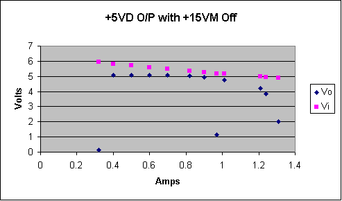
The +5VD regulator current limiting performance is studied.
Vi is the voltage from the transformer rectification/winding and Vo is that from the output of the regulator.
(R302 and 272 are 0.1R, R273 is a short and R275 2K7.)
Plot 58: Graph of the +5VD current with the +15VM turned off.
The voltage holds up until 700-800mA where the winding voltage is only 0.3V above the regulator output. At this point it follows the winding voltage until about 1.2A. Here the voltage starts to drop at a much higher rate as the curent limiting starts to work. After that the fold back kicks in at about 1.3A.
Plot 59: Graph of the +5VD current with the +15VM turned on.
With the +15VM on, the output of the +5VD is higher. In this case the current limiting and fold back is much clearer. The output of the transformer can be adjusted so this is the case for when the +15VM is off as well. The draw back is that the +15VM voltage will then be 22V when off (compared to about 16.4V) and 17V when on (compared to 15.5V). This needs to be discussed and determined which is the best way to go. The next version of the transformer may have a turn or two removed from the +15VM or added to the +5VM to adjust the voltages.
Revisit the overshoot on the +/-15VA lines on power up.
The zeners are still out, see Plots 54-57, and now another capacitor is adjusted (C78). This set on test capacitor has been in as 100n, which was found to be required to stabilize the converter before the Vaux filtering network was changed (not gone into here). With the converter now being more stable this capacitor can be reduced. The plots below show the switch on performance with different capacitor values. This capacitor filters the feedback in part of the PWM chip circuitry. Reducing it speeds the feedback up.
Plot 60: Turn on without the capacitor. Max loads. Mains power supply 1100mA at 31V. Overshoot has gone but converter switching behaviour changes so that it switches at half the rate. The switch on time of the FET is increased so that the Vaux value takes longer to come down, so the converter misses a beat so to speak.
Ch1 Yellow, +15VA.
Ch2 Blue , A Vaux.
Ch3 Pink , -15VA
Ch4 Green , +5VA regulator output.
Plot 61: Turn on with 10n capacitor. Max loads. Mains power supply 1100mA at 31V. Overshoot is under a volt. Switching performance is good for all loads. A 1n is tried which is also stable so a 10n gives atleast a factor ten clearence in perfomance.
Ch1 Yellow, +15VA.
Ch2 Blue , A Vaux.
Ch3 Pink , -15VA
Ch4 Green , +5VA regulator output.
Plot 62: Turn on 100n capacitor. Max loads. Mains power supply 1100mA at 31V. Overshoot is back.
Ch1 Yellow, +15VA.
Ch2 Blue , A Vaux.
Ch3 Pink , -15VA
Ch4 Green , +5VA regulator output.
Check board behaviour with representative switch on.
The ICU has a switch with a slow turn on to limit the inrush current to the MHC. A copy of the switch is made up and tested with the MHC power board.
Plot 63: Turn on. Max loads. Mains power supply 1100mA at 31V.
Ch1 Yellow, Switch output.
Ch2 Blue , A Vaux.
Ch3 Pink , -15VA
Ch4 Green , +5VA regulator output.
Plots 64 and 65: Turn on. Max loads. Mains power supply 1100mA at 31V. Checking the +5VD output which now shows an oscillation. This is not due to the switch but due to setting up the current limit foldback, see Plots 58 and 59. Removing the modification made in Plot 50 stops the oscilation but low loads on the +5VD line will result in the 'glitch' still being there. The oscilation seen is an interaction between the regulator and the transfomer output. When the regulator turns on the transformer ouput sinks, this turns off the regulator so the transformer output goes back up, and so on. If the load on the +5VD line will not be less than 200mA then this glitch will not occur.
Ch1 Yellow, Switch output.
Ch2 Blue , A Vaux.
Ch3 Pink , +5VD regulator output
Ch4 Green , +5VA regulator output.
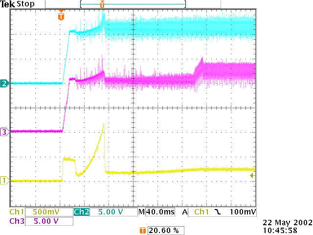
The inrush current of the power board is studied.
A 1R is put in series with the return line of the converter and a scope probe put across it. The scale will be 1Amp/Volt.
Plot 66: Turn on. Max loads. Mains power supply 1100mA at 31V.
Ch1 Yellow, Volts across 1R in main bus return line.
Ch2 Blue , +15VA.
Ch3 Pink , +5VD regulator output
Ch4 Green , +5VD winding output.
Plot 67: Turn off. Max loads. Mains power supply 1100mA at 31V.
Ch1 Yellow, Volts across 1R in main bus return line.
Ch2 Blue , +15VA.
Ch3 Pink , +5VD regulator output
Ch4 Green , +5VD winding output.
Plot 68: Turn on. Max loads. Mains power supply 1100mA at 31V.
Ch1 Yellow, Volts across 1R in main bus return line.
Ch2 Blue , Vaux A.
Ch3 Pink , Vaux B.
Ch4 Green ,
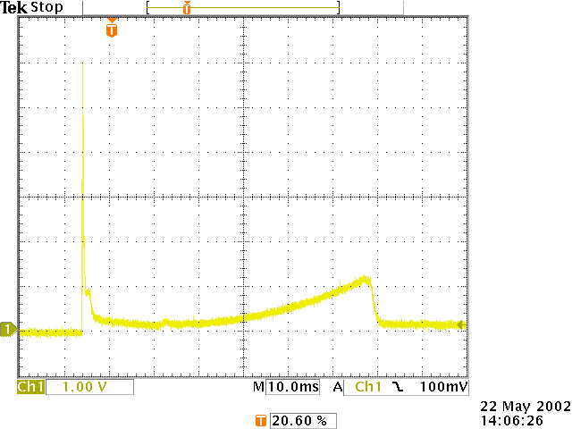
Plot 69: Turn on directly from power supply. Max loads. Mains power supply 1100mA at 31V. The effect that the slow turn on switch has can clearly be seen. The initial peak current, as the input capacitors charge up, reaches over 6Amps compared with just under 0.5Amps when the switch is in place.
Ch1 Yellow, Volts across 1R in main bus return line.
Ch2 Blue ,
Ch3 Pink ,
Ch4 Green ,
Testing continues.
Back to the Top
Back to Solar_B main page.
Last updated by Jason A Tandy 15/05/02